
Device Assessment
We identify the storage architecture, failure condition, package type and encryption risk.
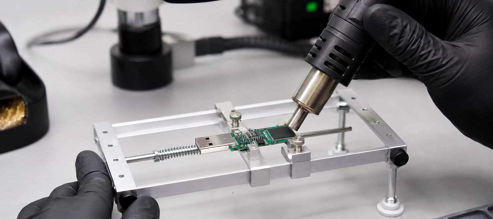
Aesonlabs provides chip-off forensics and physical flash-memory recovery for devices whose storage cannot be accessed safely through the original interface. The process can involve removing a NAND, eMMC or other surface-mounted flash package from the circuit board, preparing its contacts, acquiring its contents through a compatible reader and reconstructing the controller's data organization.
Chip-off is an advanced recovery method rather than a universal answer for every failed device. Before removing a memory package, we evaluate whether the original controller, processor or device electronics are required to decrypt or correctly interpret the stored data. When a safer controller-based, ISP, diagnostic or circuit-repair path remains available, that approach may be preferable.
A failed USB drive, memory card, camera, mobile device or embedded system normally presents data through a controller. If that controller or the surrounding electronics can no longer communicate, the flash package may still contain readable memory cells.
Chip-off bypasses the failed external interface by working directly with the storage package. After controlled removal and preparation, the chip is connected to a reader using an adapter selected for its package, pin arrangement and electrical requirements.
The first result is usually a physical or raw acquisition—not an immediately usable folder structure. NAND pages, spare areas, error-correction data, bad-block information and controller-specific organization may all need to be processed before files can be recovered.
Chip-off methods may be considered for removable, mobile and embedded storage when the package itself remains sufficiently intact for controlled removal and reading.
- USB flash drives with separate NAND memory packages
- SD, CompactFlash and other memory-card assemblies
- Cameras, recorders, drones and specialist imaging equipment
- Mobile phones and tablets with NAND, eMMC or eMCP storage
- Dash cameras, navigation units and vehicle data modules
- Industrial controllers and embedded computing devices
- Voice recorders, media players and compact consumer electronics
- Damaged circuit boards whose flash package remains intact
Package type alone does not determine recoverability. The condition of the silicon, internal bond structure, controller architecture, encryption state and availability of a compatible acquisition and reconstruction method must all be considered.
Removing a soldered memory package permanently changes the original assembly and exposes the chip to heat and mechanical stress. We therefore inspect the board, check power rails and accessible interfaces, identify the storage architecture and determine whether repair or non-destructive acquisition is possible before recommending chip removal.
This stage is particularly important with eMMC, eMCP and mobile-device storage. The package may contain an internal controller, while the device processor or security hardware may hold encryption material required to interpret the data. Preserving the original device path can be more valuable than obtaining an encrypted physical dump.
The board and package are examined under magnification before rework begins. Controlled preheating, hot-air temperature, airflow, shielding and removal technique are selected to reduce thermal shock and avoid lifting pads or stressing the package.
After removal, residual solder and contamination are cleaned from the underside. BGA and LGA packages are inspected for missing pads, substrate damage and warping; leaded packages are checked for bent, fractured or contaminated pins. Reballing or other package preparation may be required for the selected adapter and acquisition method.
A package that was damaged during an earlier removal attempt may still be evaluated, but torn pads, excessive heat exposure or substrate fractures can reduce or eliminate the available recovery paths.
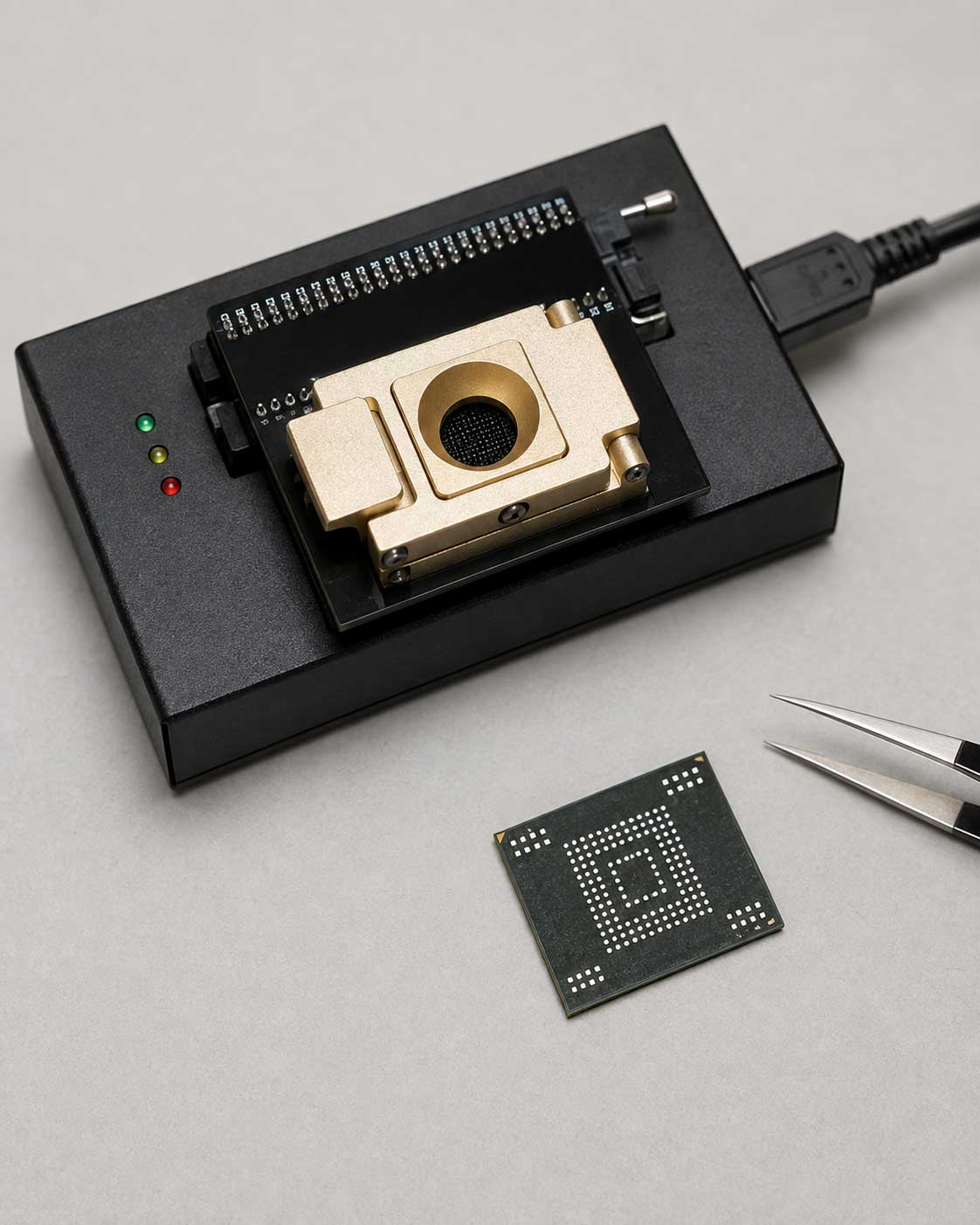
Flash packages are produced in many physical formats and pin arrangements. TSOP, LGA and BGA NAND packages require different sockets or adapters, while eMMC packages can vary by ball count, body dimensions and internal organization. Two packages that appear similar may not share the same electrical layout.
Aesonlabs uses the Rusolut Visual NAND Reconstructor platform as a primary reader for physical NAND work, together with package-specific adapters selected for the chip being examined. Supported workflows can include common TSOP and LGA packages, multiple BGA NAND configurations and appropriate eMMC adapters.
Package identification, contact condition, supply voltage and pin compatibility are verified before a read is attempted. An incorrect adapter, orientation or electrical configuration can damage an otherwise readable chip.
Once stable contact is established, the flash package is identified and acquisition parameters are configured. The reader may need to address multiple banks, chip-enable signals, dies or planes within one physical package. Voltage and read settings are selected according to the memory technology and the condition of the chip.
Weak or degraded NAND may require controlled retries, repeated passes or comparison of multiple reads. The goal is not merely to produce one dump, but to obtain the most stable and internally consistent acquisition possible while preserving the original chip.
Depending on the package and controller family, PC-3000 Flash may also be used as a complementary acquisition or reconstruction platform. Tool selection is based on the storage architecture, available reader support and the condition of the memory rather than on one fixed workflow for every case.
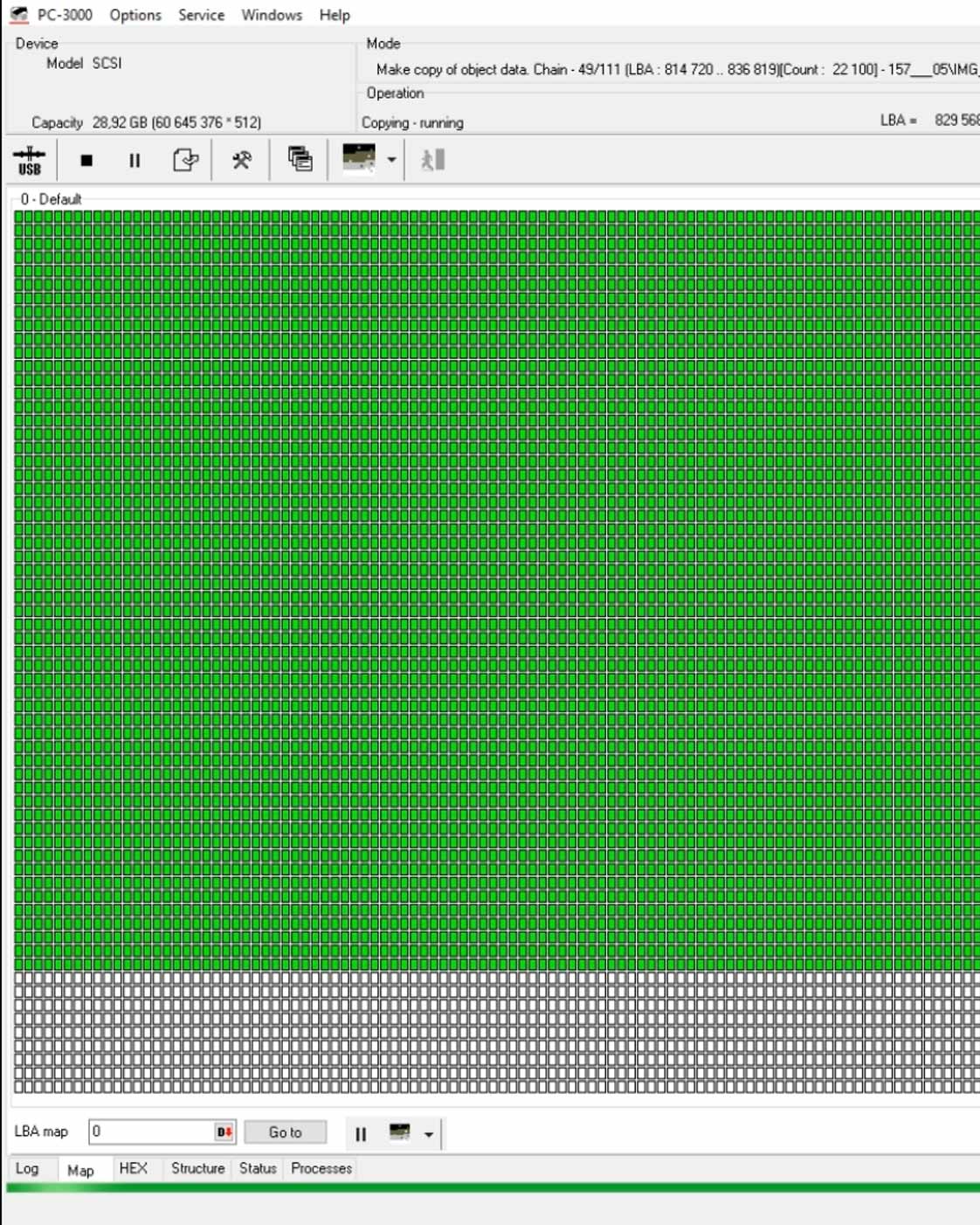
A physical read is monitored for unstable pages, uncorrectable areas, bank-selection problems and inconsistent results. Visual block maps can help identify regions that read correctly, areas requiring additional passes and sections affected by degradation.
Where possible, repeated acquisitions are compared rather than accepting a single pass without verification. Error patterns and spare-area information can provide important clues about the health of the NAND and the controller's original organization.
The acquired data is preserved as a working source for reconstruction. For forensic matters, acquisition details and cryptographic hashes of resulting images can be documented as part of the case record.
Raw NAND does not normally store user files in simple sequential order. The original controller may have distributed data across dies, interleaved pages, moved blocks, replaced defective areas and applied data transformations before writing to memory.
Reconstruction can involve separating data and spare areas, ECC correction, XOR or scrambling removal, page and block reordering, bad-block processing, interleave analysis and recreation of the controller's logical translation. The required steps vary significantly between controller families and firmware revisions.
After a logical image has been assembled, filesystems, partitions and application data can be examined. Damaged metadata may require filesystem reconstruction, database recovery or targeted file carving after the flash translation has been addressed.
Chip removal bypasses damaged electronics, but it does not bypass encryption. If the data was encrypted before being written to flash, a successful physical acquisition can still contain no independently usable files.
Some flash controllers perform hardware encryption internally. Modern mobile devices commonly use encryption keys tied to the original processor, security hardware, user credentials or operating-system state. An eMMC or NAND dump taken outside that environment does not automatically include everything required for decryption.
Controller scrambling, XOR transformations and interleaving should not be confused with cryptographic encryption; supported controller transformations can often be reconstructed. True encryption without the required keys generally cannot be overcome by reading the memory chip directly.
For this reason, we evaluate encryption risk before destructive removal whenever the device architecture can be identified. Preserving or repairing the original controller path may be the only meaningful recovery strategy for an encrypted device.
When a device is submitted for an investigation or legal matter, the physical condition of the device, identifying information and relevant handling steps can be documented. The original component is retained after acquisition, and analysis is performed from preserved working images rather than repeatedly handling the source package without need.
Chip-off acquisition can provide access to physical memory areas that were unavailable through the normal device interface, but interpretation must remain within the limitations of the storage architecture, data condition and encryption state. A raw dump should not be represented as complete or intelligible evidence until its structure and integrity have been evaluated.
- Cracked silicon or fractures passing through the memory package
- Internal bond or substrate damage within the flash package
- Severe NAND wear, charge loss or widespread unreadable pages
- Heat damage from previous uncontrolled rework attempts
- Missing BGA pads or torn package contacts
- Unsupported controller translation or undocumented organization
- Hardware-backed, controller-level or device-bound encryption
- Deleted, overwritten or trimmed data no longer present in NAND
Turnaround depends on much more than the marked capacity of the memory package. Package rework and acquisition may be relatively direct, while reconstruction of an unfamiliar controller layout can require substantially more engineering time.
- Identifying an unknown, remarked or damaged flash package
- Preparing or reballing BGA and LGA contacts
- Selecting and validating a compatible reader adapter
- Acquiring multiple banks, dies or chip-enable regions
- Repeating unstable reads and comparing acquisition passes
- Correcting ECC and analyzing spare-area structures
- Researching an unsupported controller translation
- Evaluating encryption before extended reconstruction work
A more meaningful estimate can usually be provided after package identification, initial preparation and a preliminary read. High-capacity, degraded or unsupported flash cases may require extended acquisition and reconstruction work.
Improvised heating or chip removal can destroy the only remaining copy of the data. If chip-off may be required, the original board and storage package should be preserved in their current condition.
- Do not heat the board with an uncontrolled heat gun or open flame.
- Do not pry a soldered package from the board.
- Do not grind, sand or thin a removable BGA or TSOP package.
- Do not reball the chip without documenting its orientation and package markings.
- Do not discard the original controller, processor or damaged circuit board.
- Do not assume chip-off will bypass a password or device encryption.
- Do not repeatedly power a device that overheats or has a shorted rail.
- Keep all broken pieces, shields, connectors and associated components.
Chip-off work at Aesonlabs combines board-level diagnosis, controlled surface-mount rework, package preparation, physical acquisition and controller-level reconstruction. We use professional flash-reading systems, including Rusolut Visual NAND Reconstructor and PC-3000 Flash, according to the requirements of the case.
Each device is evaluated individually. Chip removal is not recommended when a safer path remains available, and recovery is not overstated when encryption or physical NAND damage prevents meaningful reconstruction.
Customers can follow an active case through our case-management portal using the unique case number assigned when the device is submitted. Shipping options are available throughout Canada, and local drop-off is available by appointment.
When opening a case, identify the original device, explain what happened, describe any previous repair or recovery attempts and state whether the matter has legal or investigative requirements. Include the complete device and original circuit board even if the flash package appears to be the only failed component.
If the device is associated with a passcode, encrypted account or working companion hardware, preserve that information and equipment. Do not send passwords through ordinary email; secure handling instructions can be arranged after the case is opened.
We identify the storage architecture, failure condition, package type and encryption risk.
The selected NAND or eMMC package is removed and prepared under controlled rework conditions.
The package is connected through the appropriate adapter and read using professional flash hardware.
Raw pages are corrected, translated and assembled into the most complete logical result available.
Chip-off forensics is the controlled removal and physical acquisition of a flash-memory package when the original device interface cannot provide the required access. The resulting raw data must normally be interpreted and reconstructed before files or records can be examined.
No. Recoverability depends on the condition of the memory package, reader and controller support, the ability to reconstruct the data organization and whether usable decryption material remains available.
No. Chip-off can bypass a damaged interface or controller, but it cannot decrypt data without the required keys. Modern mobile and controller-encrypted devices may produce a complete physical dump that remains unusable outside the original hardware environment.
Many eMMC packages can be evaluated through compatible adapters, but successful electrical reading does not guarantee usable data. Internal controller damage, NAND degradation, unsupported organization and device-bound encryption can still prevent recovery.
NAND and eMMC packages use different body dimensions, pin counts, contact layouts and electrical configurations. The adapter must match the specific package and acquisition interface to establish safe, stable contact.
Usually not. We first evaluate whether board repair, controller-based access, ISP, diagnostic interfaces or another less destructive method can preserve the original data path.
Previously removed packages can be evaluated. Please include the original board and document the package orientation, previous heating, cleaning, reballing and reading attempts. Missing contacts or excessive heat exposure may affect recoverability.
Turnaround varies with package preparation, chip condition, capacity, number of dies, read stability and controller support. Unsupported or degraded cases can require extended acquisition and reconstruction work.
Submit the device details and describe the failure, previous work and required data. We will review whether chip-off, board-level recovery or another acquisition method is the most appropriate next step.
Submit Your Device